Hello Engineers, I hope all are well. In this article, we are going to discuss the basic architecture of the 8085 microprocessor and 8085 microprocessor pinouts along with working. So, let’s start with the introduction to the 8085 microprocessors.
Before actually moving towards understanding the architecture and pinouts of the 8085 microprocessors, we may first check on their origination history and basic features.
Introduction to 8085 microprocessor
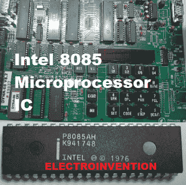
8085 is an 8-bit microprocessor that was first introduced in March 1976 by Intel corporation. It uses N-MOS technology(N-type metal-oxide-semiconductor). It is a 40 pin microprocessor IC that comes in a DIP(Dual Inline Package) package fabricated on a single LSI chip. The 8085 uses a single +5V D.C input for its operation. It requires a clock speed which is about 3 MHz.
It consists of three main sections, arithmetic and logic unit, a timing and control unit, and several registers for different purposes.
The Intel 8085A is having a clock cycle of 320 ns(nano seconds). The time for the back cycle of the Intel 8085 A-2 is 200 ns. It is having 80 basic instructions and 246 opcodes.
8085 isn’t the first microprocessor to be introduced. It was Intel 4004 to be the world’s first microprocessor which was a complete processor on a chip released in March 1971, and using cutting-edge silicon-gate technology.
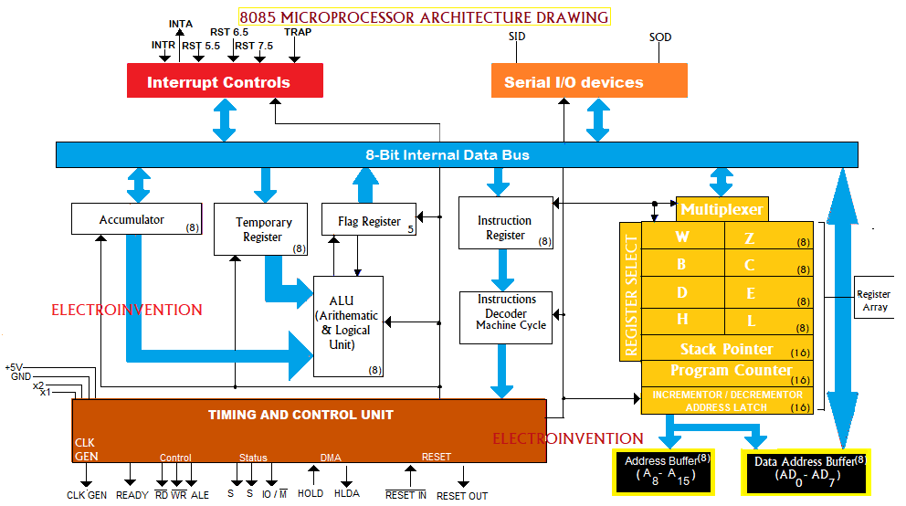
Let’s first understand the basic architecture of this microprocessor through a block diagram give here.
8085 microprocessor architecture

We will understand and discuss the physical structure and pinouts of the 8085 microprocessor after first discussing its architectural structure.
Starting with the Interrupt Controls, whenever any hardware interrupt signal is received to the microprocessor, it stops its current execution. And, now the program control is transferred to a sub-routine with the help of a CALL signal and after the execution of that sub-routine by RET signal again program control is back to the main program from where it left.
There are 5 interrupt controls, namely, INTR(least priority), RST 7.5, RST 6.5, RST 5.5, TRAP. We are going to study all of these PINs in detail later during the study of 8085 Pinouts.
The microprocessor acknowledges an interrupt and sends an acknowledgment to the peripheral that has requested through INTA.
An 8-bit internal Data Bus is connected between the IC and I/O devices. This is used to transfer the 8 bits of data at a time.
Registers are the temporary storage location to store data temporarily and manipulation of data and instructions by the microprocessor. Data remain in the registers until there is use and then erased. For eg., You guys might remember the use of variables used in programming.
Registers are of different types mentioned below:-
- 6 general-purpose registers, 8-bit, namely B, C, D, E, H, and L.
- One 16-bit stack pointer, SP
- One 16-bit Program Counter, PC
- Instruction register
- Temporary register
The Accumulator is an 8-bit register, which is connected to the ALU (Arithmetic and Logical Unit). It is used to hold the intermediate data and result of the logical operations performed by ALU during an operation. After the operation, the final result of an arithmetic or logical operation is also stored in the accumulator.
Output of accumulator is connected to the ALU.
ALU (Arithmetic and Logical Unit): ALU is the main heart of a microprocessor. This unit is responsible for all arithmetic and logical operations. Such ALU operations may include operations like Addition, Subtraction, Increment, Decrement or AND, OR, NOR, NOT on 8-bit of data.
The result is stored in Accumulator.
Temporary Register:- This is also an 8-bit register used to store the temporary data of ALU. This register is only accessible to our processor. They are of two types, W and Z.
Flag Register:- This is an 8-bit register having five 1-bit flip-flops in it. After the result is stored in Accumulator, the 5 status flags set or reset according to the result type of the operation.

Types of Flags:-
- Carry Flag (CY): It occupies the 0th, least significant bit. If the arithmetic operation results in a carry then Carry Flag is set else it is reset.
- Parity Flag (P): It occupies the 2nd bit and if the number of 1s in the accumulator is even then it is set else it is reset and it’s called even parity, and vice versa.
- Auxiliary Carry Flag (AC): It is at the 4th bit. Auxilary carry means when the carry is generated by the 3rd and passed on to the 4th.
- Zero Flag(Z): It is at the 6bit of the flag register. It is set, when the result is in 0s, else it is reset. It is also helpful to determine if two operands are equal or not.
- Sign Flag(S): It occupies the 7th (Most Significant bit). Check whether the result is of positive value or negative.
If a flip-flop for a particular flag is set, then it indicates 1. When it is reset, it indicates 0.
General Purpose Register: We have 6 general-purpose registers in our 8085 microprocessor. 6 general-purpose registers are namely B, C, D, E, H, L. Each register can hold 8-bit of data and if they work in pairs like BC, DE, HL, then 16 bit.
Instructions Register: It is an 8-bit register and it stores instructions. It holds the instructions that are to be executed. The instructions fetched from the memory are stored in this register of our uP.
Instruction Decoder: It’s used to decode the instructions from the instruction register.
Stack Pointer: It is a 16-bit special function register for holding the address of the instruction or data that are required for later processing and are stored in the stack. The stack pointer is a part of memory(part of RAM).
Program Counter: It is a 16-bit special-purpose register used to hold the address of memory location of the next instruction to be executed.
It is incremented tso that at the one execution ends and it points to the next instruction’s address in the program.
Increment / Decrement Address Latch: The address latch is 16 Bits, but 8085 holds only 8 bits of data at a time. The 16-bit increment and decrement register used to increment decrement the value of stack pinter and program counter by 1.
Increment or decrement can be performed on any register or a memory location. The 8085 requires an address bus of 16-bit wide as the memory addresses are 16-bits. We have A8-A15 demultiplexed as an 8-bit Address line and we have multiplexed address & data lines AD0 – AD8.
Timing and Control Unit:
It is a part of the CPU that generates the timing pulses and control signals for the execution. Also, it controls the flow of data between the CPU and peripherals. It controls the tuning between the microprocessor and peripherals connected to it.
Intel 8085 microprocessor pinouts

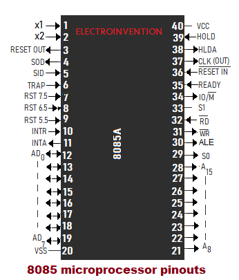
Here is the 8085 microprocessor’s pin diagram. Let’s discuss all the pins with their use and description.
- Pin 1- Pin 2(x1,x2)– The microprocessor requires the clock pulse input for operating with proper tuning with other peripherals connected to it. Pin 1 and 2 are used to connect a crystal oscillator to get clock input. In the case of 8085, we use a 6mhz crystal.
- PIN3 RESET OUT-To reset all the other device functions connected to the processor.
- PIN4 SOD– SOD is Serial Output Data line pin for serial data output.
- PIN5 SID– SID is Serial Input Data line pin, for Serial input of data. The data on this line is loaded into the accumulator on the 7th bit whenever a RIM instruction is executed.
- PIN6 TRAP– TRAP is the highest priority interrupt. It is a non-maskable interrupt, i.e it is not affected with any mask or any other interrupt.
- PIN7-9 RST5.5, RST6.5, RST7.5- These are maskable interrupts, out of these 3 RST7.5 has the highest priority.
- PIN10 INTR-INTR is the lowest priority maskable interrupt. It is an Input interrupt Request from an external device.
- PIN11 INTA‘- INTA is Interrupt Acknowledgement. It is used instead of RD during the instruction cycle after an INTR request is accepted. It is not an interrupt and is used by the microprocessor to send an acknowledgment.
- PIN12 – 19( AD0-AD7)– These are the address + data lines combined since 8085 utilize 16-bit address lines and can only hold 8-bit data so these lines are multipurpose and are bidirectional. Lower order address lines. They are multiplexed lines which are the time-multiplexed address and data bus.
- PIN20 VSS– It’s just for grounding. Connecting the negative.
- PIN21-28(A8-A15)– These are address lines and are uni-directional. Higher order address bus.
- PIN29 &PIN33 (S0and S1)– These are status pins. They specify the operation currently being performed. A small truth table can show how it works.
| S1 | S0 | FUNCTION |
| 0 | 0 | HALT |
| 0 | 1 | WRITE |
| 1 | 0 | READ |
| 1 | 1 | FETCH |
13.PIN32 RD’– PIN32 is read signal which is active low. Means when its low, then its active.Comes under the category of control signals.
14.PIN31 WR’– Write Signal, active low. Comes under the category of control signals.
15.PIN34 IO/M’– This signal tells whether the operation is a memory operation or an I/O operation. When IO/M is HIGHT(1) then it’s an I/O operation and when it’s LOW(0) it’s a memory operation.
16.PIN35 READY– Also comes under the category of control signals. This indicates that the peripheral device is ready to receive or write data. When this pin is high during any read or writes cycle.
17.PIN36 RESET IN– When this pin goes high(1), it resets the processor’s internal process. The program counter is set to 0 and the CPU remains reset condition until this pin is high.
19.PIN30 ALE– Address Latch Enable, it is at HIGH(1) when the PINS AD0-AD7 are used as address lines, else 0. When ALE is 1, then at that line the number at that time will be address and when 0, then the number that is present on the multiplexed line will be data.
20.PIN37 CLK OUT-Clock Out, output clock pin to drive the clocking of the rest of the system.
21.PIN38 & 39– HOLD(PIN 39) is a DMA signal pin. It is a signal indicating that another MASTER is requesting the use of Address and Data Buses for DMA access. PIN38 is HLDA hold acknowledgement pin, which acknowledges the DMA request. HLDA is high when t indicating that the CPU has received the Hold request and will provide the buses in the next clock cycle.
HLDA is low when request is removed.
22.PIN40 VCC– VCC pin is for +5v Dc input for the IC to get sufficient power supply to work.
8085 is now not used in computers used in this advanced era, but it’s still useful in automation(not too much) and instrumentation systems. Also , its is now moved to toy industry.
I hope you guys liked this information and will find this helpful. If you liked it you can tell in comments.
Thank You.


really very usefull articale you explane it very clearly thank you so much
Hell tushar, thanks for visiting again. Glad you liked it.
Thanks for the article ,it’s very helpful for me to understand the concept of microprocessor
.and the content is really good it’s in general and easy language to understand in just one passage of read
Thanku ❤️
Hello Manish, Thanks for visiting, and Glad you liked it.
😀